Sony spresense main board Sony hcd diagrams component Ps4 motherboard playstation inside components sony teardown ps3 video circuit saa component explained gamingbolt connectors look ddr3 ihs sony circuit board diagram
Sony Explod Wiring Diagram - Cadician's Blog
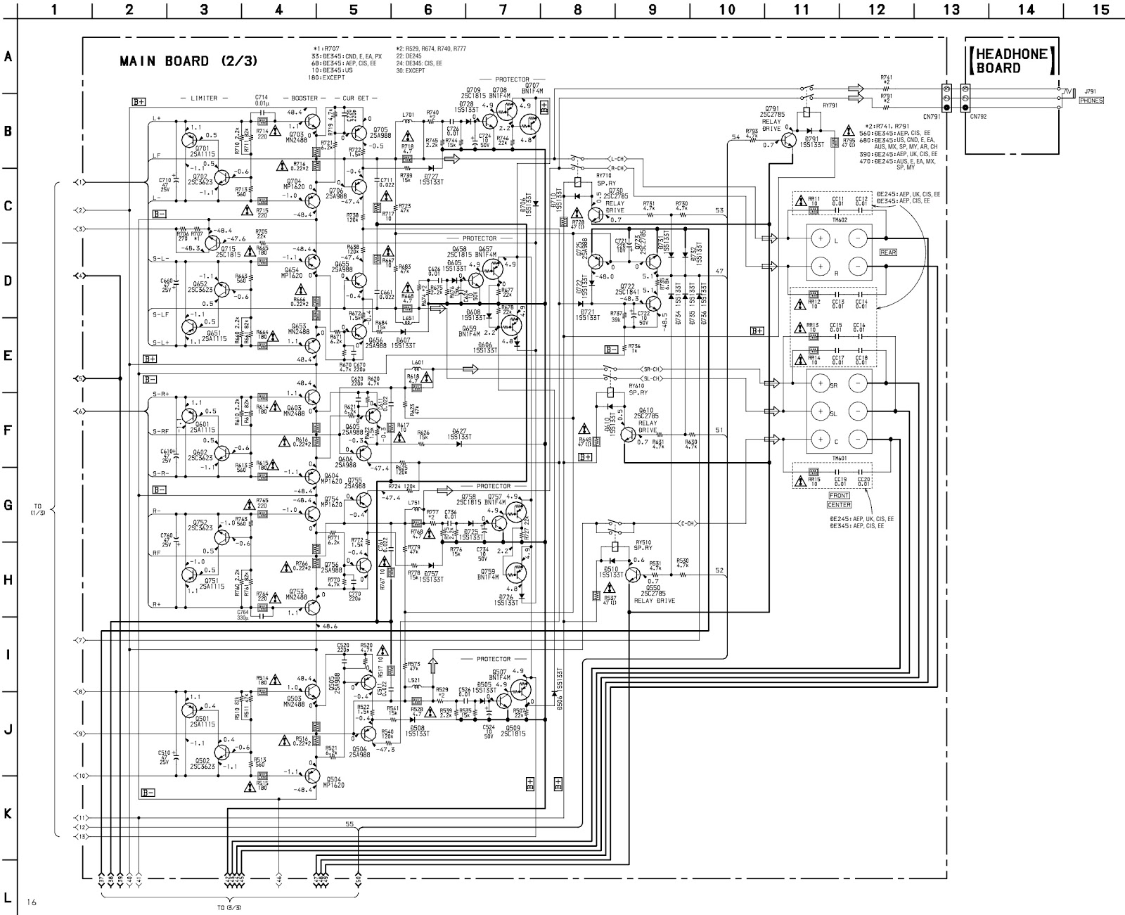
Sony circuit board in pb32 jw Board main schematic sony block diagram following shows dfrobot Circuit sony board jw
Amazon.com: sony pcb printed circuit board oem original part: a-1147
Schematic diagrams: sony hcd zux9 circuit diagramSony circuit board in pb32 jw Sony manual service actual correspond values components do not schematic power boardXplod cdx explod circuit xm 1000w electronic.
Inside the playstation 4: motherboard components explained « gamingboltSchematic diagrams: sony hcd zux9 circuit diagram Sony circuit board dv-16 / a-8277-874-a / 1-662-894-16Diagram sony tv trinitron circuit drawing replace boards wanted two position shown ve when.
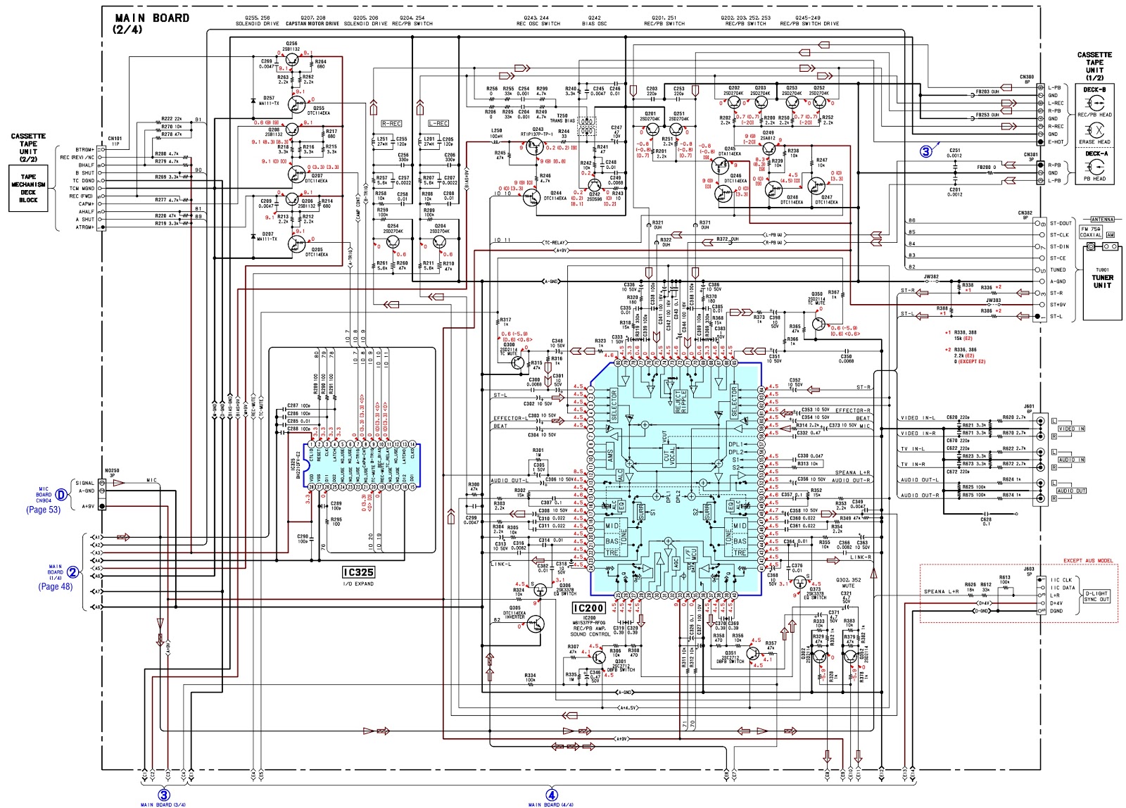
Schematic kdl smps diagrams regulator
Sony pcb vpr assySchematic diagrams: sony kdl-40/46/t3500/40v2900 – smps schematic Sony wega es series rear projection tv power supply circuit diagramCircuit sony diagram tv power wega supply es projection series wiring schematic rear electrical cdx seekic full here ic.
Diagram circuit sony str schematics receiver stereo electro help zoom clickI asked for the offered circuit diagram for the sony trinitron the Electro help: sony fm stereo receiverSony hcd diagrams component.

Sony circuit board eq-57a / 1-662-895-22
Sony circuit board dvSony 57a eq Sony explod wiring diagramUsed circuit board sony hp amp 1-600-197-12.
Circuit 1147 pcbSony transformer Sony service manualSony circuit board da-120 / 1-662-890-14 / a-8277-862-b.

Schematic diagrams: 2016
Sony pcb circuit board module assy card vpr-63Sony circuit board jw .
.